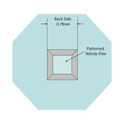
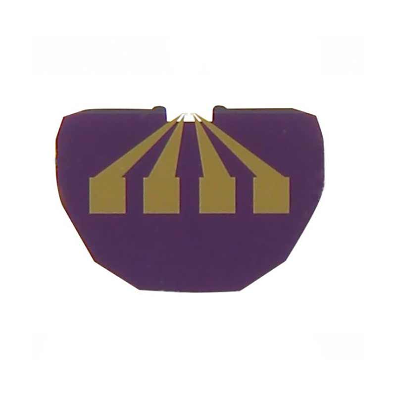
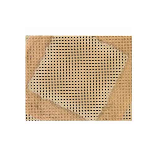
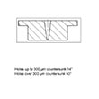
200 µm thick 3.0 mm hexagonal silicon substrate with a 0.5 x 0.5 mm aperture and 200 nm thick silicon nitride membrane with approximately 6,400 2.5 µm holes.
Low-stress silicon nitride for lift-out applications. Available with or without gold contacts.
This item is on pre-order and will take between 1-2 weeks to arrive.
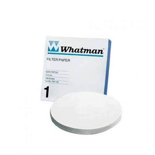
Whatman® qualitative filter papers, Grade 1 circles, diameter of 90 mm. Whatman® papers are known for being synonymous with quality, reliability, and ease of use.
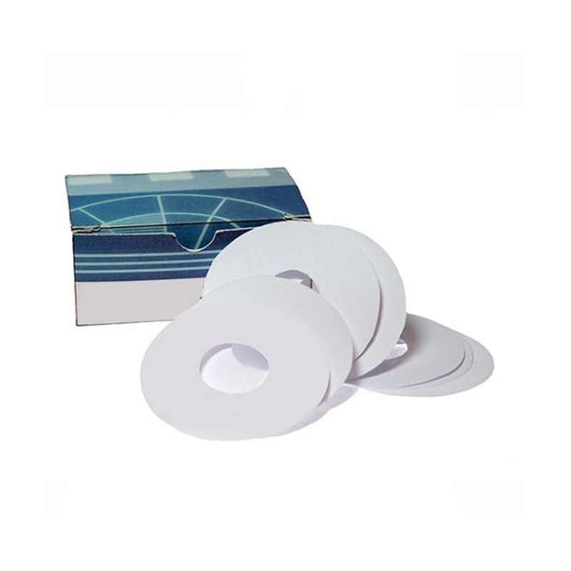
This special Filter Paper has an outer diameter of 55 mm, with an inner diameter of 20 mm. Made from Grade 595 paper.
This item is on pre-order and will take between 1-2 weeks to arrive.
Low-stress silicon nitride for lift-out applications. Available with or without gold contacts.
This item is on pre-order and will take between 1-2 weeks to arrive.
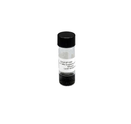
Graphene is a single atomic layer of carbon atoms tightly packed in a two-dimensional honeycomb lattice. This novel material is atomically thin, chemically inert, consists of light atoms, and possesses a highly ordered structure. Graphene is electrically and thermally conductive, and is the strongest material ever measured. These remarkable properties make graphene the ideal support film for electron microscopy.
This item is on pre-order and will take between 1-2 weeks to arrive.
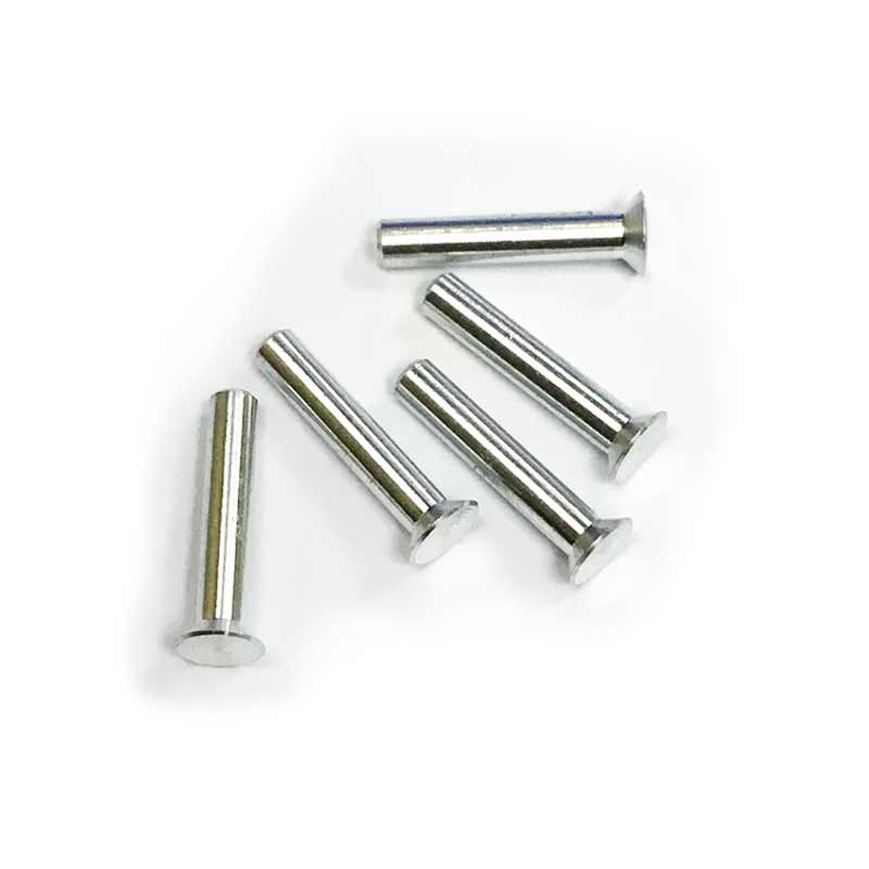
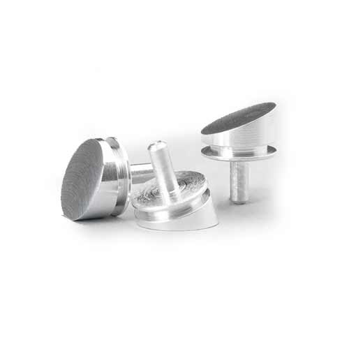
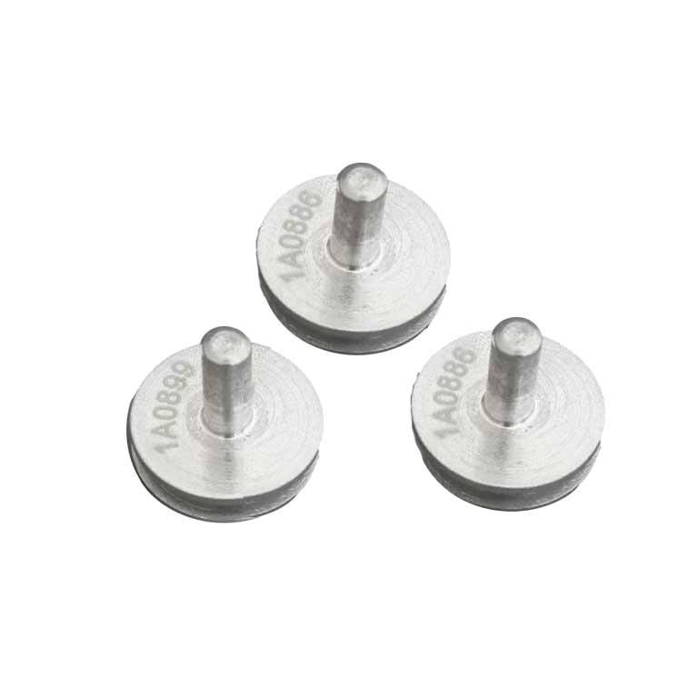
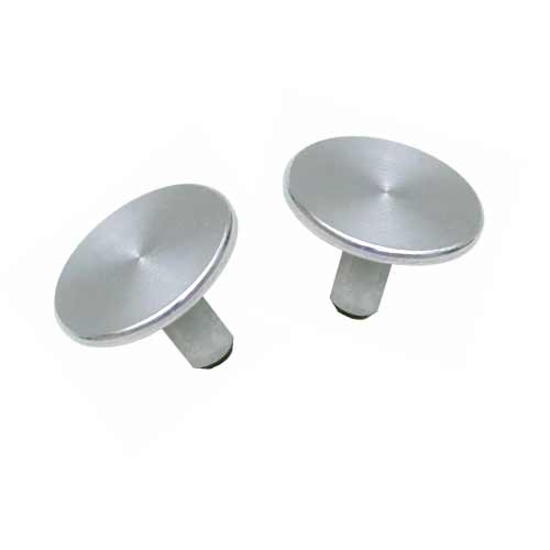
Aluminum specimen mount pin for mounting samples for ultramicrotomy. Available in two types: Slotted Screw and Bullseye.
This item is on pre-order and will take between 1-2 weeks to arrive.

FDA grade silicone rubber flat embedding moulds with a choice of cavities. Blue silicone rubber mould with 24 + 3 numbered cavities. It contains three special cavities for multiple specimen embedding.
Molybdenum Spray Aperture which can be used in Cambridge/LEO/Zeiss and Camscan scanning electron microscopes. Aperture diameter 12.68mm, thickness 0.25mm. Hole 1500um.
Please note: This item is on preorder and the current lead time is around 3 months
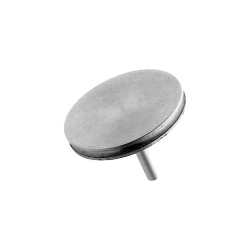
Model 70-1D with Cert Unmounted
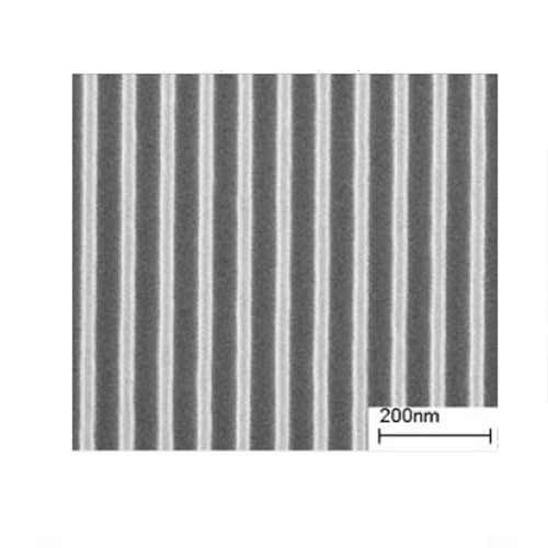
For General Purpose and Metrology Microscopes: A precision pattern providing accurate calibration in the horizontal plane for very high resolution, nanometer-scale measurements.
Period: 70 nm pitch, one-dimensional array. Accurate to +/- 0.25 nm. Refer to calibration certificate for actual pitch.
Surface: Silicon Oxide ridges on Silicon, 4 x 3 mm die. Ridge height (about 35 nm) and width (about 35 nm) are not calibrated.
This item is on pre-order and will take around 1-2 weeks to arrive.
This 78mm diameter x 12mm high aluminium stand is useful for holding stubs while mounting specimens, or to hold specimens during carbon/metal coating. Choose your type from the dropdown menu.
MAC has developed multi-element blocks of reference materials suitable for the compilation of a reference library of Auger sensitivity factors when used with the Auger Electron Microscopy (AES).
This item is on pre-order and will take around 1-2 weeks to arrive.
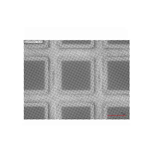
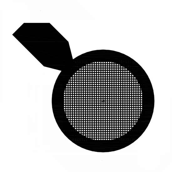
Quantifoil 2um dia (2um) 200 Mesh Copper (Pack of 10)
Circular, hole size 2µm dia, separation 2µm.

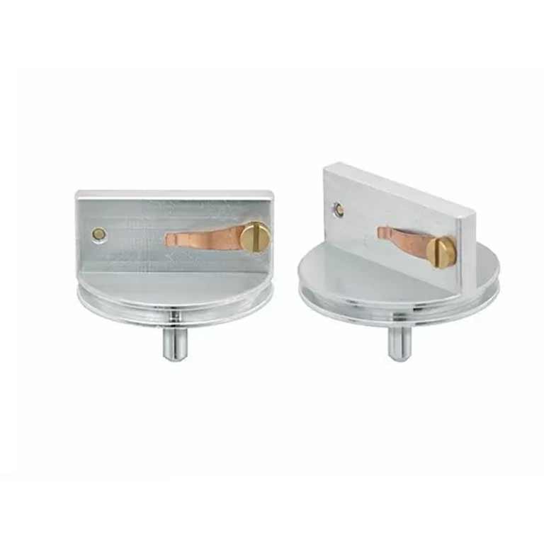
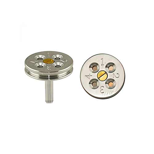
These holders with pin stub mounts accept standard metallurgical mounts.
(1.25 inch diameter). Available for microscopes using other mounts on request. Choose the size you require from the dropdown menu:
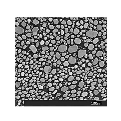
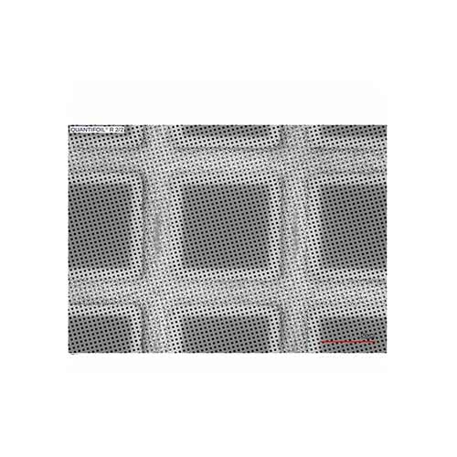
Resolution test specimen with a particle size range from approximately 5 - 150nm. Each specimen has a square grid pattern with large crystals in the centre of each grid square and very fine crystals at the edges of each grid (as illustrated).
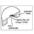
Thin film apertures are frequently used in the objective lenses of high resolution and electron beam lithography instruments. These apertures have the advantage that they heat up in the beam and are effectively self-cleaning so they minimise astigmatism.
3.04mm dia x 0.25mm thick, Hole 30um
UltrAuFoil® - ultra-stable supports for electron cryomicroscopy that reduce the movement of frozen specimens during imaging. They are made from gold which is highly conductive, nonoxidizing, radiation-hard material whose surface is chemically inert and biocompatible.
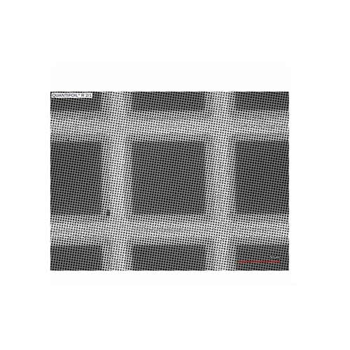
By employing a rectangular mesh the support value of the grid has been increased, offering a value intermediate between the most commonly used grid (200 Lines/") and (300 Lines/"/). Each grid rectangle is asymmetrical having different outlines in all four corners. This allows for the orientation of the grid to be determined at microscopic levels.
This item is on pre-order and will take between 1-2 weeks to arrive.
3.05mm diameter, square mesh copper TEM grids. All grids are available in 3.05mm diameter and some in 2.3mm diameter.
2mm diameter, 0.6mm thick. Molybdenum. High quality disc apertures for use in electron microscopes, Focus Ion Beam, microprobe and X-ray systems.
Assorted Aluminium SEM Specimen Stubs for LEO/CAMBRIDGE, FEI/PHILIPS, CAMSCAN, TESCAN, ZEISS instruments. 12.5mm dia, choose your type and pack size from the dropdown menu.
(LEO/CAMBRIDGE, FEI/PHILIPS, CAMSCAN, TESCAN, ZEISS, 45° chamfer. Aluminium. 10 pack)
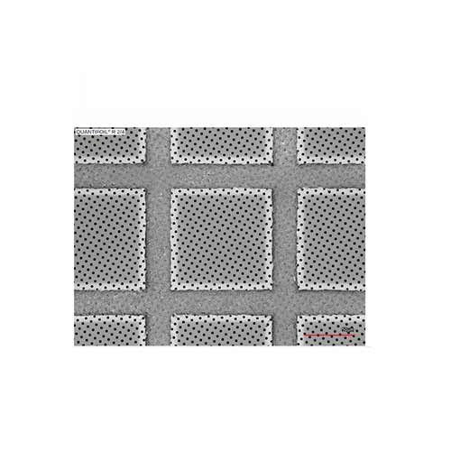
Quantifoil 2um dia (4.0um) 200 Mesh Copper - Circular, hole size 2um dia, separation 4um. This is a 10 Pack.

57mm dia x 0.1mm, Coater Type 1
A range of spare targets is available for most well known makes of sputter coaters. Before a sputtering target can be used, the preparation stage involves installation of a sputtering target into the chamber followed by pump-down of the chamber, preconditioning of the chamber and the sputtering target and burn-in of the sputtering target.
Aluminium pin stubs, 32mm in diameter. SEM Specimen Stubs for LEO/CAMBRIDGE, FEI/PHILIPS, CAMSCAN, TESCAN, ZEISS instruments. Pin length 8mm. Pack of 50.
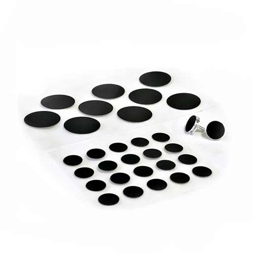
Carbon based, highly electrically conductive, double sided adhesive discs, also known as Leit tabs. These sticky discs now have an improved backing which is easy to remove and peels away cleanly. They have been developed to eliminate background noise from SEM imaging. (9mm width, Pack of 100)
Platinum Aperture 3.04mm dia x 0.25mm, Hole 5um. Platinum/iridium. High quality disc apertures for use in electron microscopes, Focus Ion Beam, microprobe and X-ray systems.
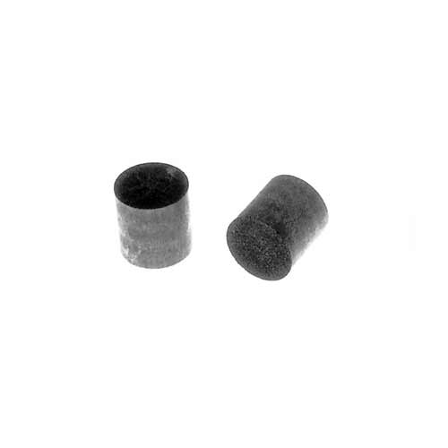
SEM Specimen Stubs, 10mm dia, 10mm high, made of carbon. Supplied individually. Other variations available, choose from the dropdown menu.
Quantifoil 2um dia (2um) 200 Mesh Copper (Pack of 100)
Circular hole, size 2µm dia, separation 2µm
Laser etched serialised standard 12.5mm dia aluminium pin stubs with pre-mounted carbon tabs, suitable for LEO/CAMBRIDGE, FEI/PHILIPS, CAMSCAN, TESCAN, ZEISS instruments.
Pin stub versions of SEMClip mounts are available in 12.5mm and 25mm diameters.
High quality replacement cartridge filaments for Hitachi (Box of 10)
10mm dia, 0.1mm thick. Molybdenum High quality disc apertures for use in electron microscopes, Focus Ion Beam, microprobe and X-ray systems.
Top hat screening apertures which can be used to reduce Xray background.
4mm dia, 0.2mm thick. Molybdenum. High quality disc apertures for use in electron microscopes, Focus Ion Beam, microprobe and X-ray systems.

Kimball Physics single crystal lanthanum hexaboride (LaB6) cathodes are available for most makes of electron microscopes and other electron beam instruments. For use in:
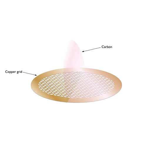
This range of carbon films has been prepared to provide a very convenient, ready-to-use specimen support. Carbon films on copper grids are thin and highly transparent to electrons, offering fine grain and low contrast that does not interfere with specimen structure.
A pack of 10 low profile aluminium flat pin stubs which accommodate specimens with small working distances in FIB applications.
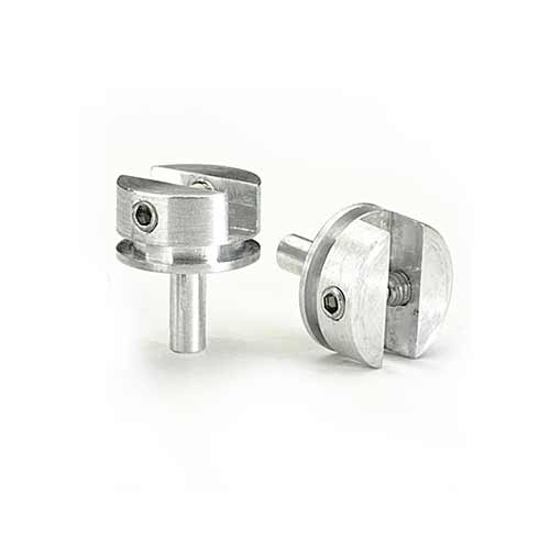
12.5mm aluminium pin stub with a slot and two grub screws, allowing specimens to be clamped for examination.(Sold as singles)
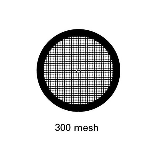
300 mesh, square pattern, 3.05mm diameter TEM grids.
Quantifoil with Circular hole, size 2µm dia, separation 1µm, pitch 3µm.
This pack is a pack of 100.
Thin film apertures are frequently used in the objective lenses of high resolution and electron beam lithography instruments. These apertures have the advantage that they heat up in the beam and are effectively self-cleaning so they minimise astigmatism.
2mm dia, 0.25mm thick, Hole 50um

This range of polystyrene particles is excellent for SEM calibration purposes. It is possible to derive an internal standard of size by mixing a suitable concentration of these particles with the particles of unknown size being studied.
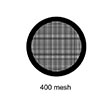
Tabbed grids offer easier handling and help to avoid contamination, allowing grids to be held securely for spraying, rinsing and drying.Square pattern, 400 mesh. Copper, Nickel or Gold.
SEM Stub (pin format) for TEM Grids which allows four TEM grids to be securely held for SEM work.

High quality replacement tungsten filaments for Cambridge, LEO, Zeiss, AEI, FEI, JEOL, Siemens, Camscan, ISI electron and TESCAN electron microscopes.

Tabbed grids offer easier handling and help to avoid contamination, allowing grids to be held securely for spraying, rinsing and drying.Square pattern, 50 mesh. Copper, Nickel or Gold.
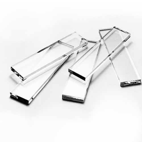
High quality glass for the production of consistent glass knives for specimen trimming, thick, semi-thin and ultrathin sectioning and cryo ultramicrotomy. 406mm x 25.4mm x 6mm (Pk 30)
3.00mm dia, 0.25mm thick. Molybdenum. High quality disc apertures for use in electron microscopes, Focus Ion Beam, microprobe and X-ray systems.

High quality replacement tungsten filaments for TESCAN VEGA series (Box of 10)
Quantifoil 2um dia (2um) 400 Mesh Copper. Quantifoils are supplied as 10 grids in this pack.
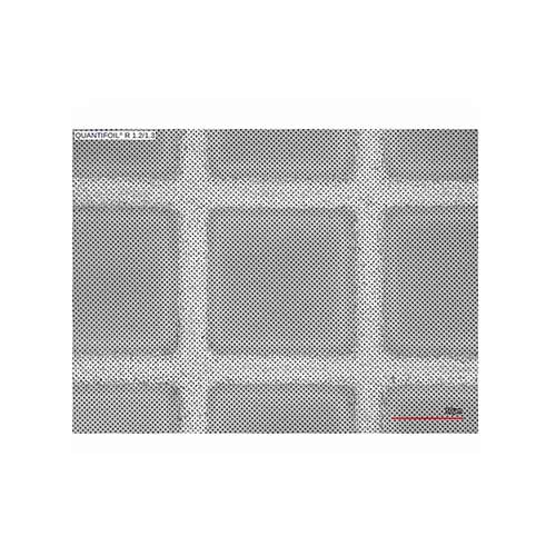
Quantifoil 1.2um dia (1.3um) 300 Mesh Copper (Pack of 10)
Circular hole, size 1.2µm dia, separation 1.3µm, pitch 2.5µm.

 PRODUCTS
 SERVICES
 SOFTWARE