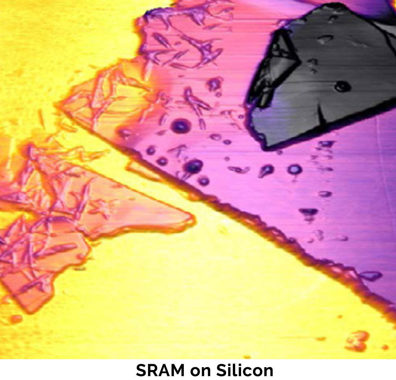
SCM measures changes in capacitance by coating an AFM probe with a conductive layer and scanning a semiconductor surface. Using microwave RF signals, it visualizes charge carrier position, doping level, and doping type, creating a two-dimensional carrier distribution map.
Key applications include determining p/n polarity of diffusion layers, evaluating diffusion layer shapes in LSI local areas, and assessing semiconductor components such as bipolar transistors, diodes, DMOS, and IGBTs.
It can also produce capacitance diagrams of CuInS₂ on silicon wafers at defective sites of semiconductor components. For SCM, tip selection should focus on conductivity, wear resistance, and stability to maintain measurement accuracy over extended scans.


 PRODUCTS
 SERVICES
 SOFTWARE